MX 7012
High resolution thickness and surface profiler for etched 300 mm silicon wafers
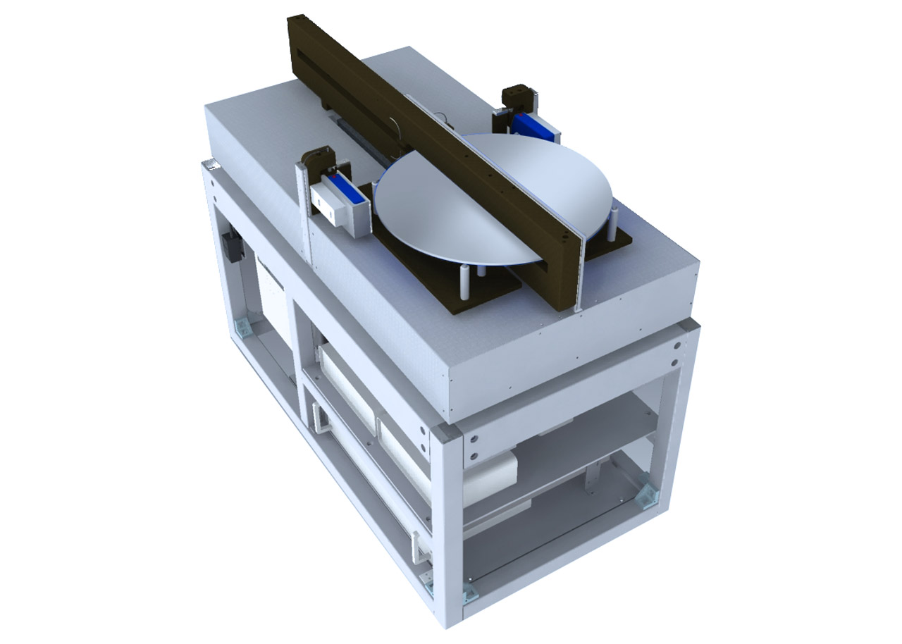
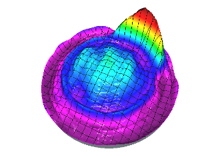
High resolution thickness and surface profiler for as-sawn 450 mm silicon wafers.
Capacitive sensors scan a diagonal cut through the center of the wafer. On the sides where the saw wire enters and exits, thickness and saw marks are measured simultaneously. (The latter with an opto-electronic measuring system.) Available asin-line integrated module or as hand-loaded stand-alone for spot checks. Comes with our powerful MX-NT operating software.
| Wafer Diameter | 450 mm |
| Thickness range | 780–970 μm |
| Software | MX-NT |
| Warp characteristics | Gravity-corrected |
You have questions, wishes or an order?
We will be happy to consult you personally.