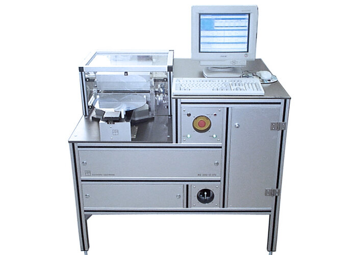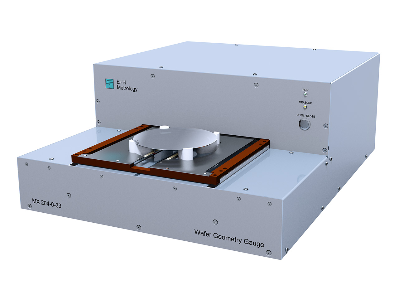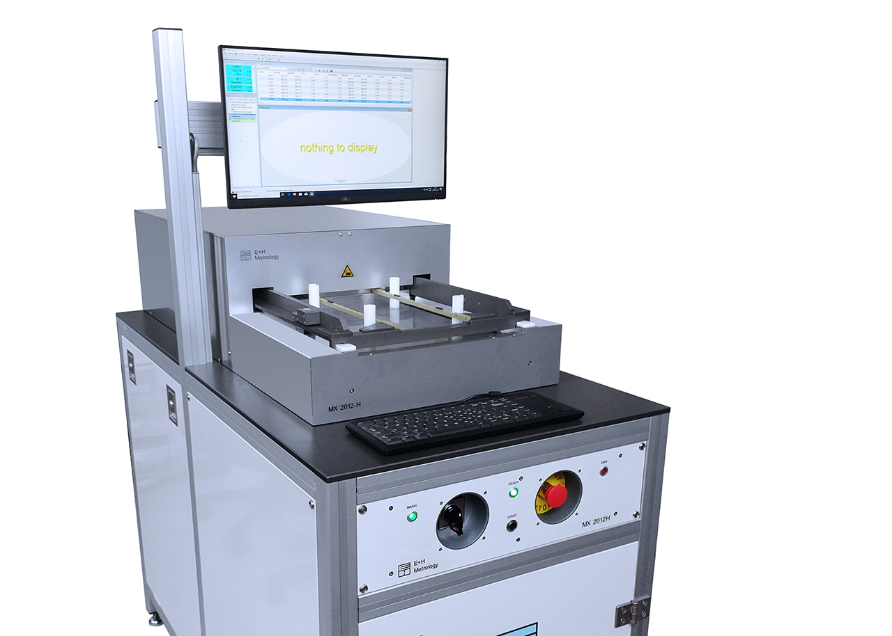
MX 2012-H
Fast chip production geometry gauge for 300 mm silicon wafers.
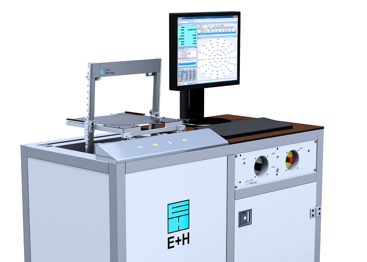
High precision chip production geometry gauge for 300 mm silicon wafers.
The MX 2012 is a automatic wafer geometry measuring instrument for 300 mm silicon wafers. This equipment is dedicated to control the wafer thickness, warp and stress between chip making processes at 69 sensor pairs. Upright position measuring avoids gravity-induced sag. Comes with our powerful MX-NT operating software.
| Wafer Diameter | 300 mm |
| Thickness accurancy | ±0.5 µm |
| Resolution | 50 nm |
| Thickness range | 500–1000 µm |
| Automatic | yes |
| Software | MX-NT |
| Warp characteristics | Gravity-corrected |
You have questions, wishes or an order?
We will be happy to consult you personally.