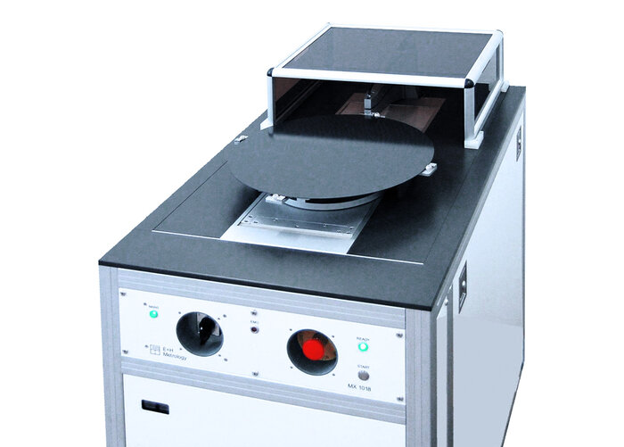
MX 102-8
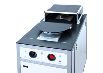
High-resolution thickness and flatness (TTV) gauge for 150–200 mm silicon wafers

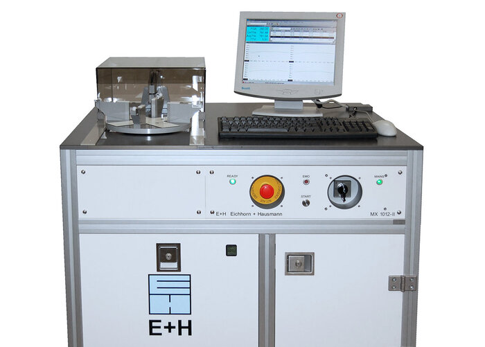
High-resolution thickness and flatness (TTV) gauge for 200–300 mm silicon wafers.
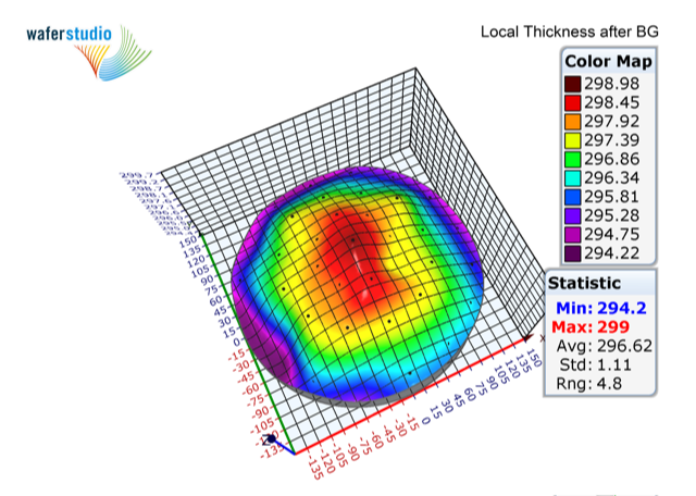
Easy adaption to different thickness ranges within a few seconds. Integration into automatic robotic sorter systems possible. The MX1012 is ideally suited for research & development, qualification of processes, and process control of thickness and flatness (TTV) especially after grinding and lapping. A pair of capacitive sensors samples four radial profiles (45 degrees) on every wafer which consist of hundreds of local thickness values. If necessary for your application, the four standard scans can be simply increased to reach an even higher measuring coverage. Comes with our powerful MX-NT operating software.
| Wafer Diameter | 200 mm, 300 mm |
| Thickness accurancy | ±0.4 µm |
| Resolution | 10 nm |
| Spatial resolution | 1 mm |
| Scans | up to 8 |
| Software | MX-NT |
| Feature |
 MX 1012 |
MX 102-6
|
MX 102-8
|
 MX 1018 |
|---|---|---|---|---|
| Wafer Diameter | 200 mm, 300 mm | 100 mm, 125 mm, 150 mm | 150 mm, 200 mm | 450 mm |
| Software | MX-NT | MX-NT | MX-NT | MX-NT |
| Scans | up to 8 | 4 | 4 | up to 8 |
| Spatial resolution | 1 mm | 1 mm | 1 mm | 1 mm |
| Resolution | 10 nm | 10 nm | 10 nm | 10 nm |
| Thickness accurancy | ±0.4 µm | ±0.4 µm | ±0.4 µm | ±0.3 µm |
You have questions, wishes or an order?
We will be happy to consult you personally.